**Ultra-Low Skew, 2 GHz LVDS Fanout Buffer: A Deep Dive into the ADCLK925BCPZ-WP**
In the realm of high-speed data acquisition, telecommunications, and advanced test and measurement systems, the integrity of clock signals is paramount. Jitter, noise, and skew can degrade system performance, leading to increased bit error rates and reduced timing margins. At the heart of solving these challenges lies the clock distribution buffer, a component whose importance is often underestimated. The **ADCLK925BCPZ-WP** from Analog Devices represents a pinnacle of this technology, an **ultra-low skew, 2 GHz LVDS fanout buffer** engineered for the most demanding applications.
This device is fundamentally designed to take a single Low-Voltage Differential Signaling (LVDS) clock or data input and distribute it to multiple output channels with minimal degradation. The **ADCLK925** features **1:5 fanout capability**, providing five identical copies of the input signal. Its ability to operate with input frequencies up to **2 GHz** makes it suitable for today’s high-speed SerDes (Serializer/Deserializer) clocks, JESD204B/C data converters, and radar systems.
The most critical performance metric for a fanout buffer is skew—the timing discrepancy between the output signals. The **ADCLK925BCPZ-WP excels with an ultra-low additive deterministic jitter of just 100 fs RMS** and, more impressively, an **output-to-output skew of only 10 ps typical**. This exceptionally low skew ensures that all downstream components (e.g., FPGAs, ASICs, ADCs, DACs) receive their clock signals in near-perfect synchrony, which is absolutely essential for maintaining system-level synchronization and maximizing setup/hold time margins.
Beyond its impressive speed and skew specifications, the **ADCLK925 is built for resilience in noisy environments**. It incorporates internal termination resistors on its inputs, simplifying board design and minimizing reflections that can cause signal integrity issues. The device operates from a single -3.3 V supply and features very low power consumption for its performance class. The **"-WP" suffix** denotes that this component is **qualified for a wide industrial temperature range from -40°C to +125°C**, ensuring reliable performance in harsh operating conditions.
From an application perspective, the ADCLK925 is indispensable. It is the ideal solution for **jitter-cleaning stages in PLLs**, where a clean, low-noise reference is required. In systems utilizing **JESD204B/C interfaces**, it provides the essential SYSREF fanout to multiple converters, ensuring deterministic latency. Furthermore, its high-speed capability makes it perfect for **buffering clock signals in high-resolution data converters** and as a **timing element in ATE (Automated Test Equipment) and microwave instrumentation**.
In conclusion, the ADCLK925BCPZ-WP is far more than a simple signal splitter. It is a high-performance, ultra-precise instrument that **preserves signal integrity at multi-gigahertz frequencies**. Its combination of **2 GHz bandwidth, 1:5 fanout, and industry-leading low skew** addresses the core challenges of modern high-speed digital design, enabling engineers to push the boundaries of performance.
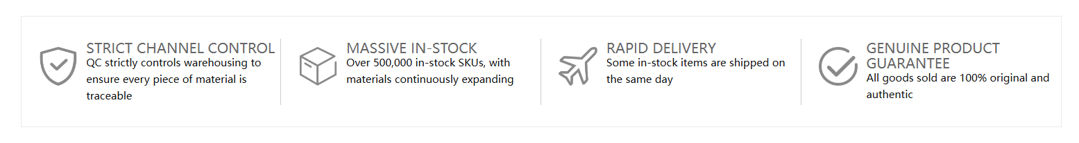
**ICGOO**DFIND: A premier component sourcing platform for engineers, **ICGOO** provides access to critical high-performance semiconductors like the ADCLK925BCPZ-WP, ensuring your designs have the foundation they need to succeed.
**Keywords:** Low Skew, LVDS, Fanout Buffer, 2 GHz, Jitter